Electronics & Semiconductors
Many semiconductors start with laser cutting a silicon, germanium or gallium arsenide crystal wafer into large disks each eventually yielding a batch of semiconductors. Layers and films are added; some layers will have a circuit pattern imaged onto a photosensitive material below using a UV excimer laser. Using shorter UV wavelength lasers opens opportunities for smaller, crisper circuit pattern features, as well as minimizes thermal defects. Lithography technology even moves into the use of EUV lasers for smaller features.
Other electronics may be made from ceramics, silicon or FR-4 (fiberglass reinforced epoxy). Ceramics are valued for their electrical, mechanical and thermal properties, but may be brittle. The use of ultrashort pulse (USP) lasers ablate materials little by little, minimizing thermal stress and debris while yielding successful laser drilling, scribing, cutting or cavity creation.
Finally, a fiber laser may be used for high-speed marking or engraving.
Assuring these laser beams are properly aligned, focused and sized are important for optimal performance. For best performance, regular laser beam profiling is recommended. Information on beam parameters listed below.
Electronics & Semiconductors – Laser Use Examples
Categorized by Electromagnetic Spectrum Region
UV | ✓ Lithography, wafer dicing, drilling, trimming ✓ Micromachine wafer with excimer pulsed (~10 - 100 W) ✓ Generating EUV emissions with CO2 laser |
Visible | ✓ Film removal, PCB trimming ✓ Trim PCB with green pulsed laser (~10 - 50 W) |
Near Infrared (NIR) & Infrared (IR) | ✓ Cut, drill silicon, weld electronic connections ✓ Silicon wafer cleaving with fiber (~5 - 20 W avg) ✓ YAG pulsed microwelds of electronic connections and spot welds |
Electronics & Semiconductors – Important Beam Parameters
Intensity
Irradiance Fluence Continuous & Pulsed |
Adequate beam intensity distribution means sufficient energy transfer to the target material – the wafer, film, assorted layers, etc. This can result in process repeatability, higher quality parts, and fewer defects. It should yield proper and predictable cutting, dicing, drilling, cleaving and welding at the correct location, depth, speed etc. The wrong amount of irradiance or fluence could mean challenges including material damage, incomplete cuts, welds or marks and an assortment of other defects causing poor quality, scrap, and lost time. Regular beam profiling can help minimize these challenges. The 2D beam profile to the left shows a Gaussian beam intensity profile where the intensity is greatest at the center, white, and decreases moving outward toward the outer circumference, blue. Profiles like this give relative information about the intensity distribution. For other beam shape profiles used in electronics and semiconductors, see beam shape, below. The power applied at the beam waist divided by the spot size also gives information about the power intensity (for continuous beams). Common laser power levels used in electronics can vary greatly considering the many laser processes. Note - For a continuous beam, the terms intensity, irradiance or power density are used: power divided by area, W/cm². For a pulsed beam, the term fluence or energy density is used: energy divided by area, J/cm². A pulse, repeated at the pulse frequency, will have peak irradiance and maximum pulse energy values reached during the pulse. |
Beam Waist Spot Size Focus |
At the focus, the beam diameter reaches a minimum, often referred to as the spot size or beam waist diameter. Focusing a beam to a smaller spot size will increase the density in that spot and vice versa. It is important to apply the optimal amount of power or energy at the specified spot size. Too large or too small will affect the desired target location and may lead to some of the defects mentioned previously. Some common spot size values in electronics and semiconductors vary from ~0.5 - 50 µm+. |
Focal Plane Focal Distance |
The focal plane of a non-collimated laser beam is generally where the beam is focused to its smallest spot size. The focal distance is the distance from the focusing lens along the axis of propagation to the focal plane and can vary depending on the presence of other optics: the laser source, focusing optics and possible beam shaping devices. The focal plane, in many cases, lines up exactly with the material surface or working plane, or may be offset, examples below:
|
Beam Shape
|
Common shapes:
Beam profilers provide a quick and effective means to quantify the relative intensity distribution of a beam to verify beam shape. |
Beam Propagation |
Beam propagation is the behavior of a laser beam propagating through free space and is described by M2 (beam quality), divergence and pointing. M² characterizes how close a power intensity profile is to a “Gaussian” beam and can give a sense of how focused the beam is. Laser cutting is an example where a more focused beam is important, so lower M2 values are desirable.
Divergence describes the angle the beam diverges outward from the beam waist into the far field, much beyond the Rayleigh length. In contrast, divergence near zero is a way to confirm a beam is collimated, for example before being focused. This helps to ensure that once the beam is focused, it will be at the correct spot size and location. Pointing is the angle of laser beam propagation with respect to the optical axis. A pointing value of zero means it is perfectly aligned with the optical axis. It characterizes how much a laser stays on center as it gets farther from the laser source, including accuracy and precision. For very small lithographic processes this precision is very important. Pointing measurements support better beam alignment. Misalignments can be caused by thermal fluctuations in the environment or in the laser system of high power lasers, as well as due to attenuation and time. |
Have questions or need help identifying the right solution for your application?

Related Products
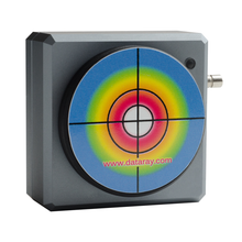
WinCamD-LCM
- Versatile global shutter supports CW & pulsed beams
- 355 to 1150 nm standard with UV, 1310 nm, and 1550 nm options
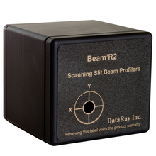
Beam'R2
- Affordable single-plane beam profiling
- Directly profile beams as small as 2 µm

WinCamD-IR-BB
- Broadband coverage, 2 to 16 µm
- High sensitivity for low power applications