Overview
CMOS and CCD image sensor technology was developed in the 1960s. Although for the last forty years CCD sensors have dominated the market, improvements in CMOS sensor design have catapulted them to a growing market share and the CMOS seems poised to replace the CCD in many applications. Often times, customers familiar with the past advantages of CCD sensors question the use of CMOS image sensors in laser beam profiling cameras. We seek to provide a short overview of the CMOS sensor’s advantages and the improvements that have enabled it to become a contender in the image sensor market.
CCD Sensors
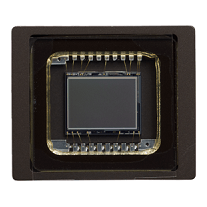
The Charged Coupled Device (CCD) sensors at their most basic level consist of an array of photodetectors. When a photon strikes the photodetector, an electron is released from the photodetector due to the photoelectric effect so that the number of electrons released from the photodetector is proportional to the number of photons (light) incident. The electrons (charge) are stored beneath the pixel in a potential well. Since the device is digital, each pixel’s charge must be converted to a digital signal. The pixels nearest the edge of the sensor transfer their charge off the sensor. Next, the pixels all transfer their charge to the neighboring pixel and once again the edge pixels transfer their charge off the chip. In this way all the charge is removed from the chip one pixel at a time. An excellent video showing mechanisms behind the CCD sensor can be seen here. As the charge is removed from the sensor it is converted into a voltage. Once the voltage is removed from the sensor, external electronics amplify the voltage and convert it into a digital signal.
CMOS sensors
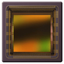
CMOS sensors initially use a similar method to detect the photons, but differ substantially from the CCD. Just like the CCD sensor, the CMOS sensor detects the light via a photodetector and the photons displace electrons via the photoelectric effect. However, once the electrons have been stored in the potential well, a different process occurs. Rather than the charge being transferred across the sensor and being read at the corner of the chip, the CMOS sensor has circuitry located at each pixel which converts the charge into a voltage (see this video for a visual representation). This voltage can then be amplified via circuitry on the sensor before being sent to the readout. Additionally, the CMOS generally has a number of channels where the voltage is read out.
CMOS Advantages
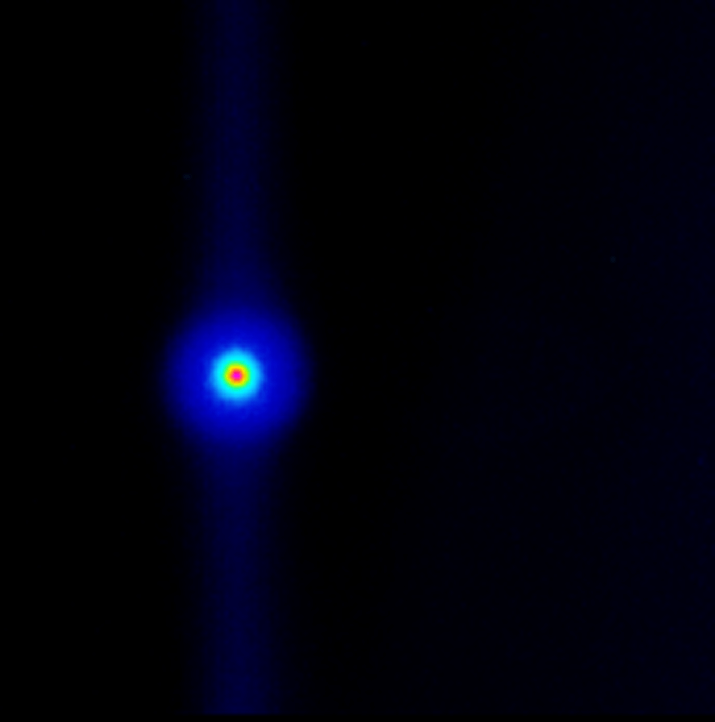
CMOS chips have several advantages that have brought them to the forefront of today’s image sensor market. CCD’s have a blooming effect that puts them at a disadvantage when compared with the CMOS sensors. When a CCD sensor has an oversaturated pixel, the charge from the pixel can fill the potential well and spill into the surrounding pixels. However, due to the architecture of the sensor, the charge can only spill along one axis and a vertical line will be seen in the image. However, since the CMOS pixels are separate and don’t transfer charge to one another, this effect is not seen in the CMOS sensors.
CMOS sensors require less power than a comparable CCD sensor and process images much faster. While CCD sensors have a limited number of channels (usually two) where the pixel data is transferred off the chip, the CMOS sensor can have an arbitrary number of channels and some sensors have as many as sixteen. The more readout channels the sensor has, the faster the sensor can process the image.
Finally, since the CMOS sensor converts the charge to a voltage at each pixel, some of the signal processing can be done with electronics on the chip. This eliminates the need for external circuitry and gives the CMOS an advantage over the CCD which requires multiple external chips for amplification and analog-to-digital conversion.
Another advantage is monetary. Although CCD sensors have special assembly lines used to create CCD sensors, CMOS sensors are manufactured with a traditional silicon chip manufacturing line and are more economic. Due to the low cost of chip manufacturing, and the high volume of image sensors that are used in today’s mobile devices, image sensor manufacturers have invested heavily in CMOS sensor improvement.
CMOS vs. CCD
For many years CCD chips were the predominant sensor used. One of the foremost reasons behind CCD use was their lower noise level, but in recent years, advances in CMOS technology have steadily reduced the CMOS noise floor. The multichannel readout of the CMOS lowers the bandwidth of each channel and reduces transfer noise. Another former CCD advantage was the global shutter in which every pixel records the light at the same time. In the past, CMOS sensors were exclusively manufactured with a rolling shutter. One row of pixels would detect light, then the following row etc. Although for many applications the rolling shutter poses no problem, laser profiling cameras often record data from pulsed lasers. For short pulses a rolling shutter only records the illumination of some pixel rows, while others are dark. Recently, image sensor manufacturers have created CMOS sensors with a global shutter, thus enabling their use in pulsed laser profiling applications.
DataRay's Laser Beam Profiling Cameras
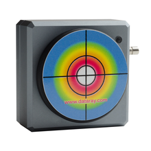
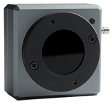
In the past DataRay cameras exclusively utilized CCD image sensors. However, with the continuing development and improvement of CMOS image sensors, DataRay has begun to incorporate the CMOS sensors into our camera product line. Our newest camera, the WinCamD-LCM, uses a 1-inch CMOS sensor to provide accurate and reliable beam profiling measurements. The CMOS sensor used is state-of-the-art with a global shutter and a large surface area.
The full range of cameras we offer along with our scanning-slit profilers can be found on our website. Should you have any questions about the sensors used in our cameras, feel free to contact us.
